Staying ahead of the competition is a major issue for product designers in today's cutthroat business conditions. The onus rests on the shoulders of system designers to develop novel, distinctive offerings.
In this regard, incorporating new, high-density designs into products is an effective innovation method. Thus, a power designer's primary focus should be on optimizing for maximum efficiency, maximum reliability, and minimum footprint.
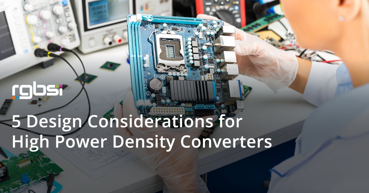
With that, here are 5 of the most notable design elements to be aware of for high power density converters.
1. Thermal Management and Thermal Design Optimization
High-density power supply designs have unique requirements for thermal management.
Due to the limited surface area available for dissipating the heat produced by the power converters and maximum permissible safe operating temperatures, the thermal management issues in such designs are becoming increasingly tough. For instance, wasted heat inside the casing from the worst-case power dissipation imposes a limitation for thermal management. With the power supply getting smaller, efficiency must be a priority to avoid overheating the casing.
Moreover, while a high-density architecture is great for conversion efficiency, it may cause a bottleneck in thermal performance. Dissipating the same amount of power in a smaller area is unsustainable. Component dependability and failure rates are of greater concern when operating temperatures get elevated.
In this regard, lower-profile power metal-oxide-semiconductor field-effect transistors (MOSFETs) placed on the top side of the PCB improve thermal performance with convective airflow because they do not get shadowed by taller components like the inductor and electrolytic capacitors.
2. Gate Driver Design
For the most part, gate drivers are found in any power converter. Controllers cannot reliably open and close the power switch promptly due to the low voltages required by the control circuitry. Therefore, the controller sends signals to the gate driver, which can handle significantly more power and can, thus, operate the MOSFET's gate as required.
Elements of a circuit are subjected to large voltage fluctuations and high currents when functioning in high-power or high-voltage applications. Due to the high voltages and currents inherent in the power conversion circuit, a current leakage from the power MOSFET to the control circuitry may easily trigger a severe breakdown of the control circuit by frying the transistors.
A gate driver isolation can fix this. Capacitive isolators in this system get made up of two capacitors connected in series. The dielectric is silicon oxide, which is built into the silicon die. These capacitors can handle high voltage peaks without breaking.
3. Component Design
Increases in switching frequency, essential for shrinking passive filter components, can only be achieved through technological advances in component design.
Improvements in silicon and packaging for power MOSFETs are one example; the emergence of gallium nitride (GaN) power devices with extremely low parasitic capacitances is another. While power semiconductor performance has increased, magnetic component performance has also increased, although at a slower pace. Last, you may often adjust the switch-node voltage slew rate without power-draining snubber or gate resistor components because of the control IC's thoughtful layout, which includes integrated, adaptive gate drivers adjacent to the MOSFETs.
4. EMI Performance
Power supply engineers also have to worry about electromagnetic interference (EMI). There must be adequate margins between the conducted and radiated EMIs and the global regulatory requirements. EMI shielding is also important for ESD & EOS protection.
EMI compliance testing is a significant milestone. EMI filtering often has little room in a high-density layout. A compact design lessens radiated emissions and boosts resistance to interference. Essential measures include minimizing loop areas with high di/dt currents and lowering surface areas with high dv/dt voltages.
5. PCB Layout
Power system designers should learn and master PCB design. Although engineers sometimes outsource layout to specialists, they are ultimately responsible for reviewing and approving the design.
Conclusion
Increasing the efficiency of power converters saves energy, reduces the end user's impact on the environment, improves reliability, and brings down total cost of ownership. In the end, using these design considerations can give you a leg up on the competition with product design of high power density converters.
About RGBSI
At RGBSI, we deliver total workforce management, engineering, quality lifecycle management, and IT solutions that provide strategic partnership for organizations of all sizes.
Electrical & Electronic Services
We offer state-of-the-art services that fully integrate electrical and electronic design through manufacturing. With a “think forward” outlook, clients’ use our team of experts to ensure their products, systems, and processes are always current and compliant in the most efficient way possible.
Learn more about electrical & electronic services.

.png?width=60&name=Struggling%20with%20EV%20Development%20Key%20Engineering%20Challenges%20and%20Solutions%20(21).png)
.png?width=60&name=Struggling%20with%20EV%20Development%20Key%20Engineering%20Challenges%20and%20Solutions%20(19).png)
.png?width=60&name=Struggling%20with%20EV%20Development%20Key%20Engineering%20Challenges%20and%20Solutions%20(18).png)
.png?width=60&name=Struggling%20with%20EV%20Development%20Key%20Engineering%20Challenges%20and%20Solutions%20(14).png)
.png?width=60&name=Struggling%20with%20EV%20Development%20Key%20Engineering%20Challenges%20and%20Solutions%20(11).png)
.png?width=60&name=Struggling%20with%20EV%20Development%20Key%20Engineering%20Challenges%20and%20Solutions%20(10).png)
.png?width=60&name=Struggling%20with%20EV%20Development%20Key%20Engineering%20Challenges%20and%20Solutions%20(9).png)
.png?width=60&name=Struggling%20with%20EV%20Development%20Key%20Engineering%20Challenges%20and%20Solutions%20(8).png)