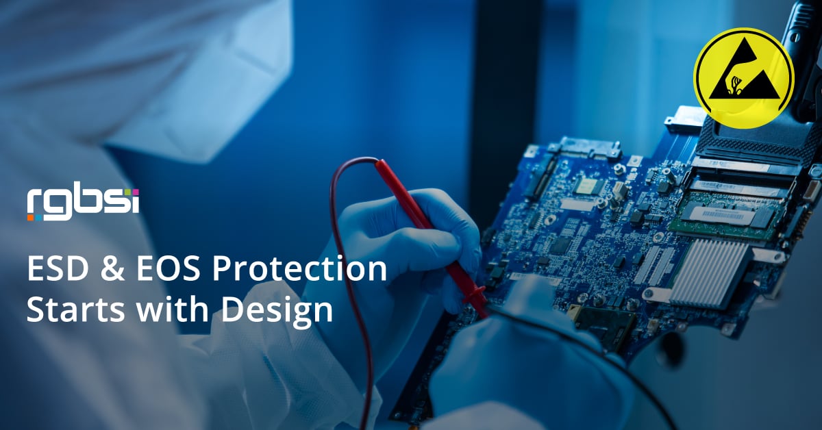
Static electricity can build up on many things, including the human body: It only takes one careless touch to damage or completely ruin a piece of electronic equipment severely. Thus, circuit protection is crucial in safety-critical designs.
This article will discuss the importance of design in ESD & EOS protection.
Defining ESD & EOS
Electrostatic discharge (ESD) is the temporary flow of electric current between two electrically charged objects or devices due to contact, an electrical short, or a dielectric breakdown.
Another phenomenon that shares similarities with electrostatic discharge is electrical overstress (EOS). EOS describes a condition in which too much voltage, current, or power is being applied to a device, causing it to malfunction.
Damage from ESD and EOS can manifest as a variety of failure characteristics or visible indicators of damage to the component. Burns, overheating, shorts, and open circuits are all potential warning indicators.
Building ESD & EOS Verification into the Electronic Design Flow
Verifying ESD and EOS protection in an intricate IC design is a difficult undertaking. This section explains the stages of IC development and provides some instances of ESD, and EOS checks performed at each stage.
Phase 1 – Product Definition
The requirements for ESD performance and the product's design define the need for ESD components and cells. Appropriate ESD cells get defined for each pin application node based on these functional specifications.
Based on the available design data during this design phase, you can conduct the following ESD checks:
- Protected device verification for the specified design functional specifications
- Cell-level verification of the current ESD cells
- Package-level verification
Phase 2 – Architecture
Chip architecture's functional or behavioral level at this design stage becomes defined. Then, the required ESD components and library cells get identified.
Like the previous section, you can conduct the following ESD checks:
- Protected device verification
- Cell-level verification
Phase 3 – Design
This phase is the heart of the design process, wherein all other product teams engage in complex ways. There are three distinct stages within it.
First, chip architecture modules, digital I/O, and power banks are floor planned. Under this stage, you can conduct the following checks:
- Protected device verification for the digital modules
- Cell-level verification for the new ESD library cells
- Intra-power domain verification for the digital intellectual property (IP)
- Floor plan or top-level ESD verification
- Package-level verification
Second, physical designs for the analog (and RF) modules and associated I/O banks get developed at this point in the design process. The following ESD checks could get run using the provided design information:
- Cell-level verification for the analog pin ESD library cells
- Intra-power domain verification for analog pad rings
- Intra-power domain verification for each analog module
- Inter-power domain verification
- Protected device verification for the individual modules
- Special ESD rule verification
In the last phase, the IP and I/O for the entire chip are integrated, along with the packaging. The following ESD checks could get done using the available design data:
- Inter-power domain verification
- Package-level verification
- Protected device verification for the full IC
Phase 4 – Qualification
Final design audits and ESD performance assessments can get carried out in this phase using the verification findings from the earlier phases. This phase frequently gets carried out by a unique, business-defined standard practice methodology that gets outlined in an "ESD/EOS checklist'' or other documents.
How to Design Against ESD/EOS in Electronics?
Because of the potential damage that ESD and EOS can do to electronic devices, protecting them from these risks is essential to ensuring their normal functioning. Here are key tips to prevent ESD/EOS.
Safeguard Entry of Discharge
Always use static-safe containers for carrying and storing items to prevent accidental discharge. Until they reach static-free workstations, static-sensitive components should remain sealed in their packaging.
Protection Diodes
Most engineers utilize transient voltage suppressor (TVS) diodes for overvoltage protection.
TVS diodes are connected in parallel to shield a circuit. When induced voltage surpasses avalanche breakdown voltage, diode resistance drops. So, it diverts the surplus energy to the ground, preventing current from flowing to the protected IC.
Reduce Electrostatic Charge Generation
Static electricity can damage machinery and other production aids, but grounding can eliminate this problem. For items made of insulating materials, you may need to use ionization or apply a topical antistatic to stop electrostatic charges from forming and building up.
Conclusion
While there are many potential sources of electrical damage, improving circuit reliability can be achieved by integrating the appropriate circuit protection components and solutions. In the end, protecting devices well against ESD/EOS events makes them more reliable, which saves companies that create new products considerable resources.
About RGBSI
At RGBSI, we deliver total workforce management, engineering, quality lifecycle management, and IT solutions that provide strategic partnership for organizations of all sizes.
Electrical & Electronic Services
We offer state-of-the-art services that fully integrate electrical and electronic design through manufacturing. With a “think forward” outlook, clients’ use our team of experts to ensure their products, systems, and processes are always current and compliant in the most efficient way possible.
Learn more about electrical & electronic services.


.png?width=60&name=Struggling%20with%20EV%20Development%20Key%20Engineering%20Challenges%20and%20Solutions%20(8).png)
.png?width=60&name=Struggling%20with%20EV%20Development%20Key%20Engineering%20Challenges%20and%20Solutions%20(7).png)
.png?width=60&name=Struggling%20with%20EV%20Development%20Key%20Engineering%20Challenges%20and%20Solutions%20(3).png)
.png?width=60&name=Struggling%20with%20EV%20Development%20Key%20Engineering%20Challenges%20and%20Solutions%20(1).png)
.png?width=60&name=Your%20How%20Digital%20Engineering%20Reduces%20Product%20Development%20Time%20by%2040%25%20text%20(1).png)


